For a long time, I made “homebrew” panels: it works, but between alignment, finish, and repeatability, you quickly lose time — and precision. With this method, the aim is a clean, consistent result: accurate drilling, and above all a process that’s reproducible from one module to the next, without specialised tooling, using accessible computer-based tools.
In this tutorial, I walk through my front-panel process step by step, to get a tidy aesthetic, a simple workflow, and a panel that lands right first time.
Software used:
- Front Panel Designer
- Illustrator (You can use Inkscape)
- Kicad
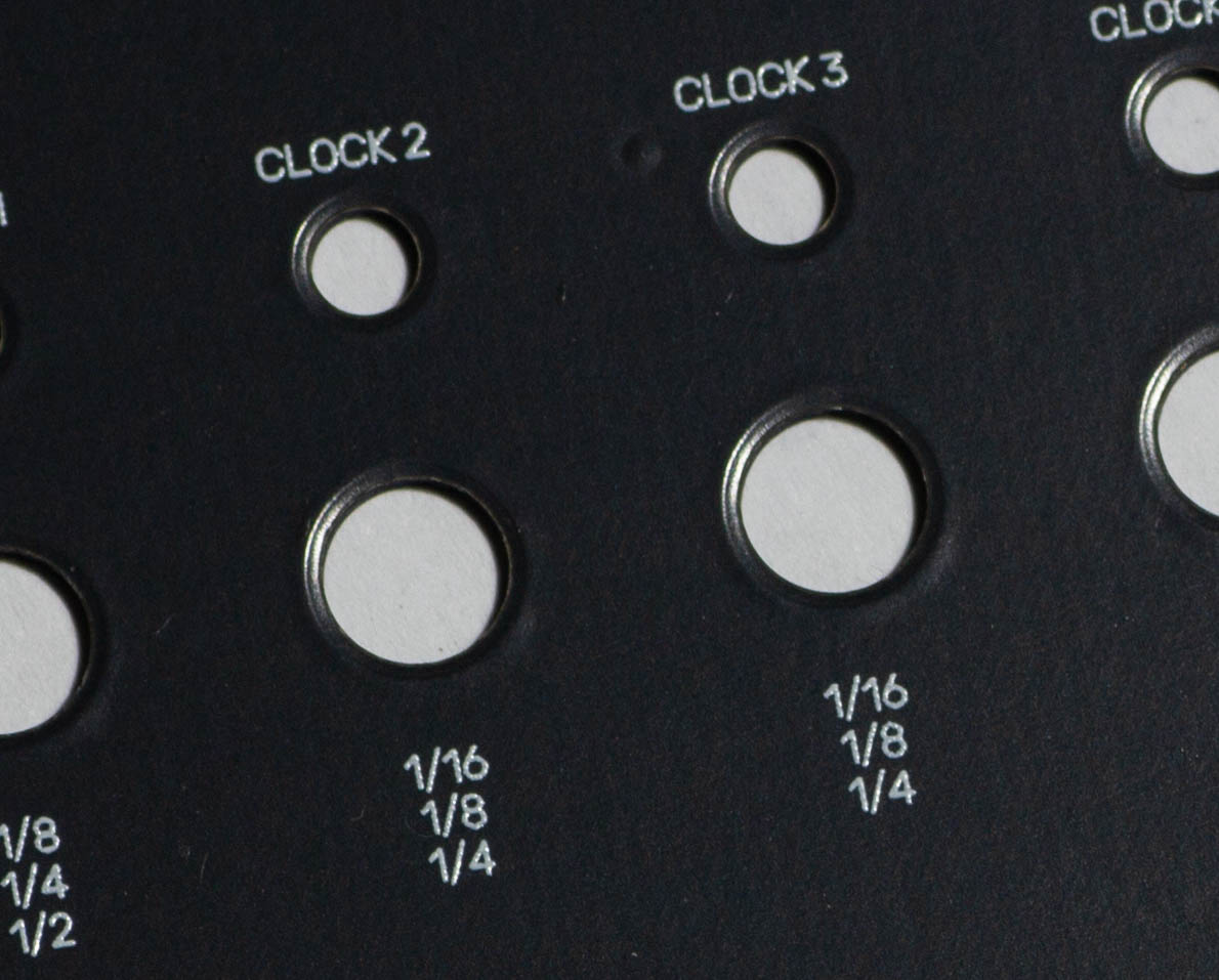
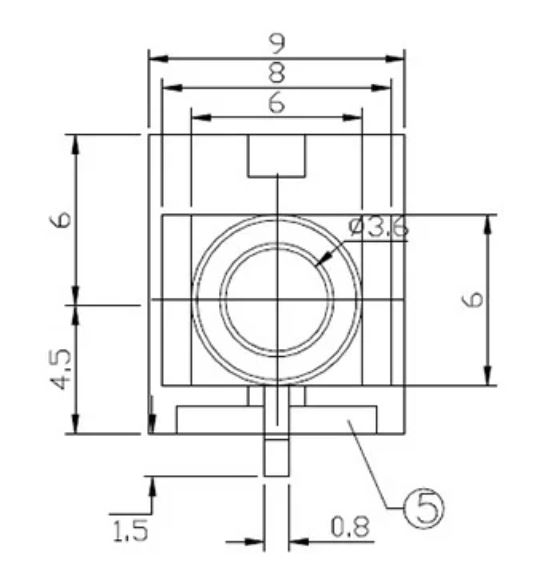
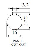
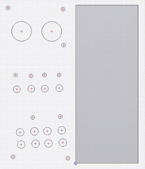
Step 1: I start by listing all the front-panel components (potentiometers, jacks, switches, LEDs, etc.) and noting the recommended drill diameter for each one, based on the datasheets.
Step 2: Next, I define the panel format. For the width and the mounting-hole positions, I follow the Doepfer standards — to stay Eurorack-compatible and avoid any surprises during installation.
Step 3: Then I work out where everything should go on the front panel (pots, jacks, switches, LEDs…), thinking first about real-world use: ergonomics, finger space, patch cables that won’t get in the way of controls — and of course the diameter of the knobs I plan to use, to avoid any overlap.
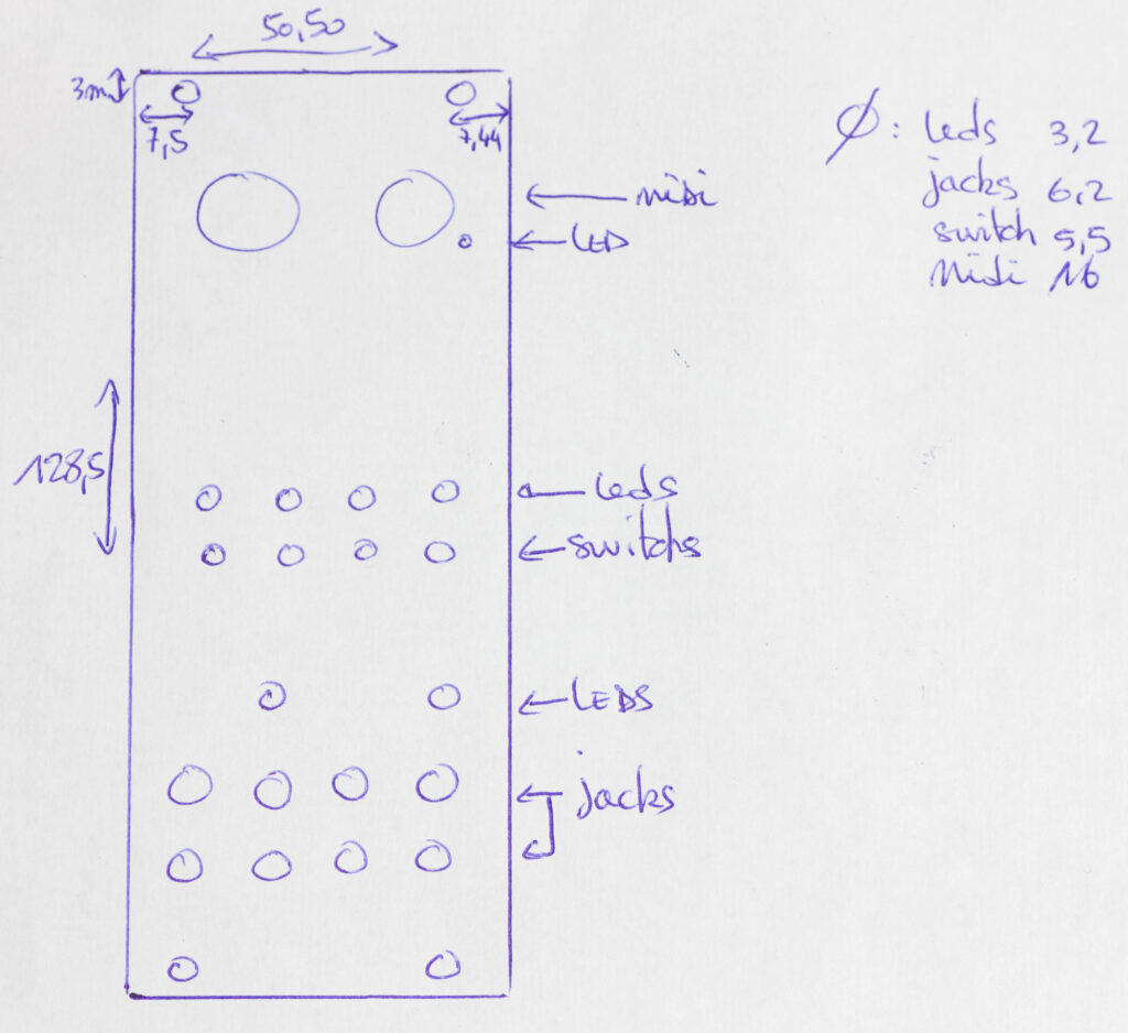
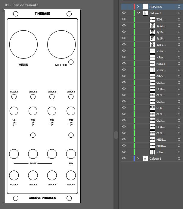
Step 4: I then place all the drill holes in Front Panel Designer. Once the panel layout is final, I export a .DXF file and import it into KiCad (on the Edge.Cuts layer) to line up the PCB, and into Illustrator to prepare all the graphics.
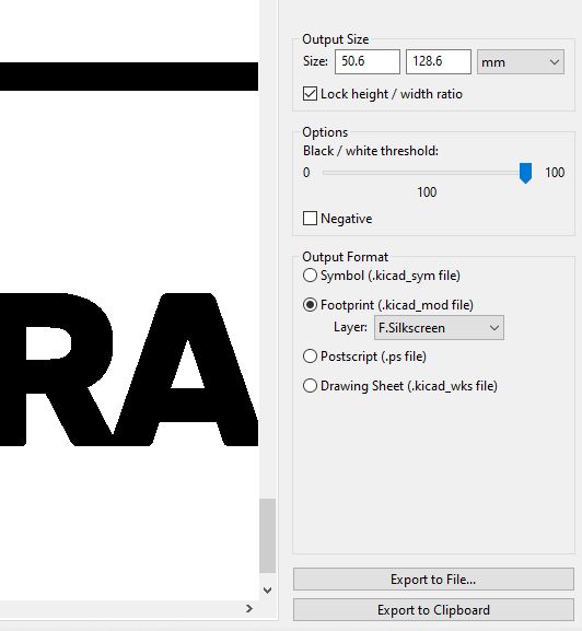
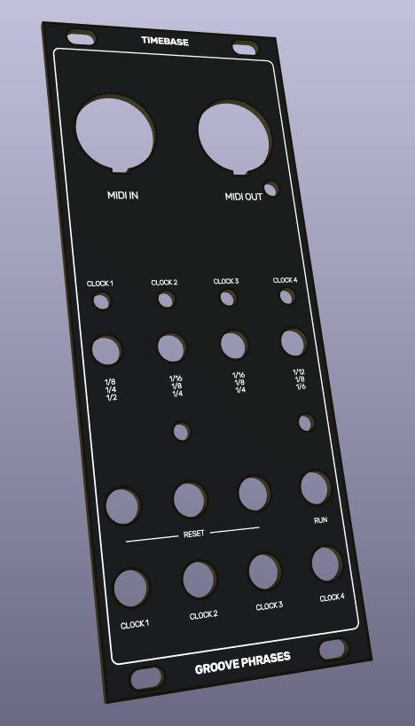
Step 5: In Illustrator, I add a dedicated layer and build the panel graphics: control labels, inputs/outputs, switches, LEDs, the module name, and sometimes an illustration. I always keep the real knob size and the space around each element in mind, so everything stays readable once the module is assembled and patched. When everything is in place, I export a .BMP at the maximum resolution.
Step 6: In KiCad’s Image Converter, I open the .BMP, set the threshold (100% for pure black and white), then export the result to the clipboard so I can paste it straight into the PCB editor.
Step 7: In KiCad’s PCB Editor, I paste the design (Ctrl + V) onto the Front Silkscreen layer, then position it precisely using the previously imported Edge.Cuts outline as a reference.
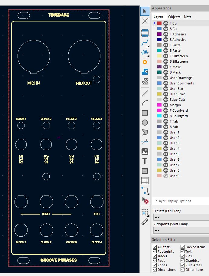
Step 8: Next, I draw the ground plane on both sides (top and bottom), pulling it as close as possible to the outer edges of the panel so it follows the panel shape.
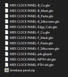
Step 9: Finally, I export the Gerbers and drill files, following the manufacturer’s recommendations. I bundle everything into a .ZIP archive and upload it — with one last check along the way (outline, holes, silkscreen, alignment) to make sure everything is clean before starting production.
In the end, it can look like an overcomplicated “factory” on paper, but in practice the workflow is very straightforward: once the template is in place, each new panel comes together quickly, cleanly, and — most importantly — in a perfectly reproducible way. You’re limited to a single silkscreen colour, but that’s more than made up for by accurate drilling, impeccable alignment, and a professional finish.
Examples: Timebase, Envelocity.
Leave a Reply